Productos
CY7C68013A USB Development Board
Sistema de desarrollo para el chip CY7C68013A. Posee interfaz I2C/ISP, y puerto USB. Asimismo brinda un puerto de expansión GPIO. Se alimenta con 5v.
COD: HTHR0214-156A
Peso: 0.014 Kg
Disponibilidad: Sin Stock
ARS 21394.00
El producto no está disponible para la venta en este momento
Características
Features:
1, using CY7C68013A-56 chip: low-power version of the enhanced 51-core, 16KB program data areas, frequency of 48Mhz, 480Mbps high-speed transmission protocol standards, in line with USB2.0 specification, backward compatible with USB1.1.
2, firmware, EEPROM: Complete in-system programming solution with a USB cable directly to download firmware, on-board to provide 16K (24LC128) a large program memory (EEPROM), used as storage VID / PID and the USB firmware, the program space to meet the CY7C68013A needs.
3, all the GPIO pin through the 2.54mm standard leads to very convenient for learners to expand their own design.
4, with the appropriate board firmware can be achieved through the core function of the logic analyzer
5, PDF format, provide the schematic and the Related information.

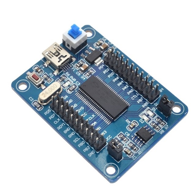
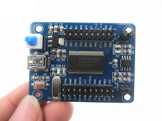
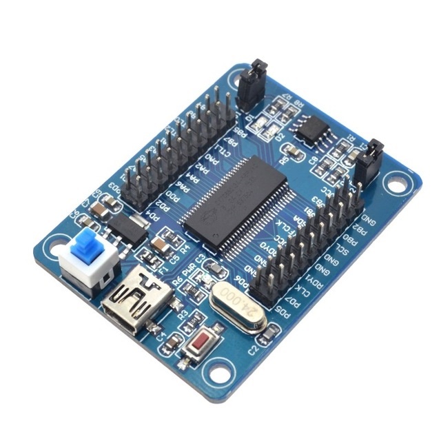
CY7C68013A is a development board, with CY7C68013A-56PVXC microcontroller as the main control chip which is an enhanced revision of 8501 integrated chip; it has an integrated IIC controller. In addition, it is perfectly functionally compatible with USB2.0_USB_IF communication by connecting with USB cable. (Read more in CY7C68013A-56PVXC data book.
This development board can provide power supply and establish communication connection with USB cable, the stabilivolt AMS1117 provides 3.3v for master control, all the pins of CY7C68013A-56PVXC are broken out to be connectors, making it easy for the connection of peripheral circuit and with other modules; for the measuring and testing of pins. Furthermore, AT24C128 chip and relevant circuit are designed for this development board, program can be uploaded into AT24C128 through USB, and you can read and write by controlling the jumper cap (plug in the jumper cap, AT24C128 closed, pull it off, AT24C128 opened),which effectively make up for the lack of ROM storage in CY7C68013A-56PVXC,making it a more perfect CY7C68013A-56PVXC learning board.
Overview and Hardware Resources:
1.A USB interface.
2.A bunch of extension port.
3.A power indicator.
4.A jumper that controls the open and close of data memory read and write of AT24C128.
5.A power switch.
6.A reset button.
7.Weight: 14g.
8.Size: 55mm*42mm*10mm.
Interfaces:
- Interface Layout:

- Interface specifications:
USB interface: For circuit board power supply and the uploading program for CY7C68013A. Extension IO port: all the pins of CY7C68013A are broken out as connectors in the form of header, Power switch: for the open and close of power supply to the PCB through USB interface Reset button: reset the main.
Jumper Instruction:
Jumper cap of 24C128: controlling the ability of data reading and writing. Plug in the cap, AT24C128 is closed; remove it, AT24C128 is started.
Jumper cap of D1, D2: controlling the power of LED light. Plug in the cap, the anode of LED 1 and 2 will be connected to the positive pole of power source through resistance. Remove the cap, the anode of D1 and D2 will be open.
Interface Connecting and Setting
Connect the CY7C68013A to computer with a USB cable when performing functional test for it.
Link:
http://www.geeetech.com/wiki/index.php/CY7C68013
SDK:
Media:CY7C68013Adevelopment board.rar